https://www.tadalive.com/blog/....157337/construya-su-
Beğen
Yorum Yap
Paylaş


https://www.tadalive.com/blog/....157337/construya-su-
https://www.whizolosophy.com/c....ategory/politics-gov
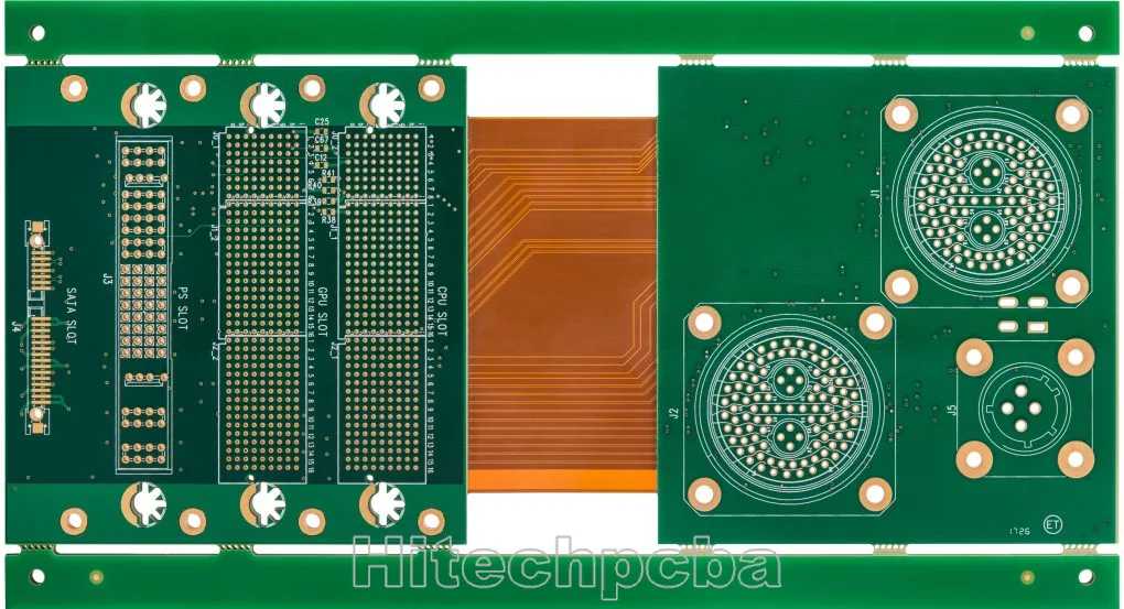
Rigid flex pcb board
Hitech Circuits Co., Ltd is a professional rigid flex pcb printed circuit board manufacturer & supplier from China, our rigid-flex pcb board saves production time, minimize product size and improve equipment reliability, suitable for mobile phones, digital cameras, medical devices, smart control system, and other smart smart devices. If you are looking for long term rigid flex pcb and other pcb products partner in China, Hitech is the right company you are looking for, don’t hesitate to contact salesHitech Circuits Co Limited.com if you need any help from us.
Rigid flex PCB board fabrication
Rigid-Flex Printed Circuit Board
Rigid flex PCB board fabrication
Rigid-flex PCB China (10 layers)
Rigid-Flex Printed Circuit Board
Rigid-flex PCB China (10 layers)
Rigid flex pcb board China ( 2 layers )
PCB Products, Rigid-Flex Printed Circuit Board
Rigid flex pcb board China ( 2 layers )
6 layers Rigid-flex PCB
PCB Products, Rigid-Flex Printed Circuit Board
6 layers Rigid-flex PCB
Flex rigid printed circuit board 10 layers
PCB Products, Rigid-Flex Printed Circuit Board
Flex rigid printed circuit board 10 layers
6 layers flex-rigid printed circuit board
PCB Products, Rigid-Flex Printed Circuit Board
6 layers flex-rigid printed circuit board
What is rigid flex pcb board?
Rigid-flex PCB board, it is a circuit board that combines flexible and rigid circuit board technology in the application. Most rigid-flex boards are composed of multiple layers of flexible circuit boards, which are attached to one or more rigid boards from the outside and/or from the inside, depending on the design of the application. The flexible substrate is designed to be in a constant deflection state, and is usually formed as a deflection curve during rigid flex pcb manufacturing or assembly.
Hitech rigid flex pcb manufacturing process
After the production of FPC flexible boards is completed, the production of Hitech rigid flex pcb boards can be completed through the following processes.
1. Punching
Drill holes on FR4 and PP film, and the design on the alignment hole is not the same as the general through hole. After the punching is completed, browning is required.
2. Riveting
Laminate copper clad laminates, PP adhesives, and FPC circuit boards and place them neatly. The original old process is to laminate and pressing step by step, but it is a waste of time. After many attempts, we found that the stacking process can be completed once.
3. Laminate
This is a relatively complete step in the production of rigid-flex pcb board. Most of the materials are integrated for the first time. First, the bottom layer is copper clad laminate and PP film, above are the FPC flexible board produced in the previous process, and a PP film is placed on the FPC flexible board, then place the last layer of copper clad laminate. All materials to be laminated are placed in order and pressed together.
4. Trimming
That is to remove the part of the circuit board where there is no circuit at the edge of the circuit board currently and in the future. Afterwards, it is necessary to measure whether the material has excessive expansion and contraction. Because the PI used in the production of flexible boards is also expansion and contraction, this has a very large impact on the production of circuit boards.
5. Drilling
This step is the first step to turn on the entire circuit board, and the production parameters should be produced according to the design parameters.
6. Desmear
First, remove the scum generated by the drilling of the circuit board, and then use plasma cleaning to clean the through holes and the board surface.
7. Immersion copper
This step is the process of electroplating through holes, also known as hole metallization. Realize through-hole power conduction.
8. Plate plating
Partially electroplating copper on the upper surface of the electroplating hole makes the copper thickness above the through hole exceed a certain height of the copper clad board surface.
9. Outer dry film positive film production
The same as the production process of the anti-corrosion dry film of the FPC board, the circuit to be etched on the copper clad board is made. After the development is completed, check the circuit.
10. Graphic plating
After the initial copper sinking, pattern electroplating is performed, and the current time and copper plating wire are used according to the design requirements to reach a certain electroplating area.
Elan Imperial Sector 82 Gurgaon presents a cutting-edge commercial project, located strategically in the bustling Sector 82 of Gurgaon. This development offers prime spaces designed to elevate businesses to new heights. With its contemporary architecture and top-notch amenities, Elan Imperial sets a benchmark for commercial excellence in the region. Whether you're launching a startup or expanding a corporation, these versatile spaces cater to diverse business needs. The project's proximity to key infrastructure ensures convenience and accessibility, making it an ideal choice for entrepreneurs and investors looking to thrive in Gurgaon's dynamic business landscape.
Read More. https://affordablehomegurgaon.....com/property/elan-im
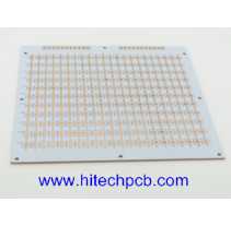
Metal Core PCB
Metal Core PCB, MCPCB Manufacturing Service
What is aMetal Core PCB?
Metal core aluminum PCB is an aluminum-based copper clad laminate with good heat dissipation function. Generally, the single layer aluminum-based PCB is composed of a three-layer structure, which is a circuit layer (copper foil), an insulating layer and a metal base layer. Also used for high-end use is designed as a double sided and multilayer aluminum PCB.
A metal core PCB is a special PCB having a metallic base layer. This base layer is usually made of aluminum or copper. As it contains a metallic layer, it is named Metal Core PCB (MCPC.
An aluminum PCB is a printed circuit board that contains a thin layer of conductive dielectric material. They are also called aluminum cladding, aluminum base, MCPCB (metal clad printed circuit board), IMS (insulated metal substrate), thermal conductive PCB, etc. Aluminum PCBs were developed in the 1970s, and soon their applications increased sharply. The first application is their use in amplifying hybrid integrated circuits. They are being used on a large scale, so we must understand aluminum PCB and its importance.
The metallic layer present in the metal core PCB does many wonders along with the dielectric layers. These PCBs are far better than FR-4 PCBs in terms of bearing thermal and pressure stresses. They are suitable for extreme conditions and high heat-dissipating components. Therefore, it has solved many issues that were faced in other PCB substrates. Metal core PCBs have tons of benefits, but all of them come at an additional cost.
What is IMS Circuit board ?
Insulated Metal Substrate (IMS)
The use of IMS circuit boards for simple single-layer circuits is a special but very effective method of heat dissipation for components across circuit boards. These generally consist of aluminium supports, insulation layers and copper foil. The base materials are available in different design versions.
Aluminum pcb Applications:
LED technology: Illuminated signs, displays and lighting
Automotive industry: LED headlights, engine control and power steering
Power electronics: DC power supply, inverters and engine control
Switches and semi-conductor relays
Aluminum pcb Manufacturing process
The metal core PCB fabrication process is ①Grinding plate (500# brush)→②Washing→③Passivation→④Washing×3→⑤Blow-drying→⑥Drying. Grinding plate: Grinding the iron surface only, grinding the plate according to FR4 parameters.
Metal core PCBs must follow a particular process due to the presence of the metal layer in the stackup. If the board is a single-layer board with no layer transitions back to the metal plate, then the standard FR4 dielectrics can be used, where the dielectric layer is pressed and bonded to the metal plate.
For multilayer dielectric stackups, the metal core must first be drilled to allow for a layer transition without creating a short circuit. First, slightly larger holes are drilled into the metal layer, and the holes are plugged with an insulating gel. This gel is cured and hardened, allowing it to be plated with copper, just like a standard via. The rest of the stackup is pressed and bonded with the metal layer, and through-holes are drilled through the stackup, followed by plating and cleaning.
The first board must check the circuit without scratches, black tin surface, other defects, and uniform wear marks.
Why Choose us for Metal core PCB ?
Competitive Cost for PCB Manufacturing
We offer high-quality customized PCB Boards with reasonable cost and the best service because we know the cost is significant to a product’s success. We have cost control for each process to provide reasonable PCB costs for our customers.
The reason why we can provide you with low-priced PCB manufacturing services is that we have a very complete supply chain management system and maintain a perfect and solid cooperative relationship with suppliers, and through mass procurement and mass production to reduce costs to a greater extent to customers so that you enjoy lower prices than the same industry, higher than the quality of the same industry.
Free DFM PCB Design Checking
We have a professional engineering team to provide complete engineering support for customers. Free DFM helps to save cost and reduce potential problems during PCB (printed circuit board) manufacturing.
Ten professional PCB engineers with over 20 years of PCB experience, with rich experience in various industry standards and process quality requirements, provide customers with optimized design PCB solutions at the design-in stage.