What is Heavy Copper PCB?
Heavy copper PCB is a circuit board with a copper thickness that is ≥ 3oz per sq. ft in its outer and inner layers. What makes a circuit board classified as a heavy copper PCB is its thicker plating. During the production of heavy copper PCB, copper thickness is enhanced through plated holes and sidewalls. For instance, when a PCB has 2 ounces of copper per sq. ft thickness, it is a standard PCB. However, if it has more than 3oz of copper, it is a heavy copper PCB. Heavy copper PCB is considered a reliable wiring option. Heavy copper PCB is different from extreme copper PCB which features within 20 oz to 200 oz per sq. ft.
What does Heavy Copper PCB offer?
Heavy copper PCB has a lot to offer. It has got some unique features that make it an ideal option for high-end applications. Let’s discuss some of the benefits of this PCB; Great thermal distribution: Due to its copper-plated vias, this PCB offers high thermal resistance. Heavy copper PCB are used in applications that demand high speed and high frequency. You can also use this PCB at harsh temperatures. Mechanical strength: Heavy copper PCB feature great mechanical strength. When this PCB is used, it makes the electrical system durable and robust. Good conductor: Heavy copper circuit boards are a good conductor. They are utilized in the production of electronics due to this feature. They help to link various boards together. These boards can transfer current.

How is Heavy Copper PCB Fabricated?
For the fabrication of heavy copper PCB, plating or etching is often used. The main aim is to add copper thickness to sidewalls and plated holes. The methods used in fabricating heavy copper PCB aren’t far-fetched. Heavy copper PCBs need special etching and plating methods to ensure the extra thickness of copper. Using the normal etching techniques for the fabrication of heavy copper PCBs isn’t ideal. Normal etching methods produce over-etched margins and edge lines that are uneven. PCB producers now use advanced etching and plating methods to achieve straight edges.
Heavy copper PCBs are produced via etching and plating methods. The major aim in the production of this PCB is to add copper thickness through sidewalls and plated-through holes. Heavy copper PCBs have several benefits which make them in high demand. Due to their outstanding features and benefits, they can meet your electrical requirements. These circuit boards will always dissipate heat generated due to heavy currents conduction. Electronics using heavy copper boards have been in use for a long time. Heavy copper can carry high currents. These boards will continue to meet the needs of various applications. High power circuit wirings can be developed using Heavy Copper PCBs. Such a wiring mechanism offers more reliable thermal stress handling and offers fine finishing while incorporating multiple channels on a single layer of a compact board.
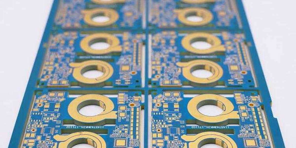
Printed circuit boards (PCBs) are usually bonded with a layer of copper foil on a glass epoxy substrate. The thickness of the copper foil is usually 18μm, 35μm, 55μm, and 70μm. The most commonly used copper foil thickness is 35μm. Domestic copper foil thickness is generally 35 ~ 50μm, there are thinner than this such as 10μm, 18μm; And thicker than that like 70μm. The thickness of composite copper foil on 1~ 3mm thick substrate is about 35μm. The thickness of the composite copper foil on the substrate less than 1 mm thick is about 18μm, and the thickness of the cladding copper foil on the substrate thicker than 5mm is about 55μm. If the PCB copper foil thickness is 35μm, printed line width is 1mm, then every 10mm long, its resistance value is about 5mΩ, its inductance is about 4nH. When the di/dt of the digital integrated circuit chip on the PCB is 6mA/ns and the working current is 30mA, the noise voltage generated by each part of the circuit is estimated to be 0.15mV and 24mV according to the resistance value and inductance value of each 10mm printed line. Heavy Copper PCB boards can be made simply by combining two main processes: electroplating and etching. Compared to other PCBs, the circuit is made of a thin layer of copper foil. The copper plates are uniformly laminated with FR4 or other epoxy-based substances. The average weight of a Heavy Copper PCB can be 4 oz. (140μm), which is a better ratio than a copper-shared PCB. Let's look at the benefits.

Heavy Copper PCB Manufacturer Circuit board Assembly – One-stop service Printed Circuit Boards (PCB) are usually coated with thick copper foil on a glass epoxy substrates commonly thickness of copper foil are 18μm, 35μm, 55μm, and 70μm. The most common copper foil is 35μm. The heavy copper PCB boards can simply be manufactured by two main processes plating and etching in the combine. As compared to other PCBs, the circuit is made of a thin layer of the Copper foil sheet. The plates of copper are laminated uniformly with FR4 or other epoxy-based substance. The average weight of the thick copper PCB weight could be 4oz (140μm), and this ratio is better as compared to another type of PCBs who have copper in common. Let’s check out the benefits of it.
Benefits of Heavy copper PCB Fabrication
Here are some of the advantages of heavy copper PCB, let’s follow them:
1. Favorable circumstances of Heavy Copper PCB
2. Plating innovation in overwhelming copper permitted a mix of plating and carving which causes in straight sidewalls and immaterial undercut.
3. The substantial copper plating creates high-current circuits and control circuits that watches the profoundly thick and straightforward whiskers’ structure.
4. This empowers the board fabricator to build the measure of copper thickness in plated gaps and by means of sidewalls.
5. The blend of substantial copper results on a solitary board called PowerLink.
6. The substantial copper in the PCB likewise encourages in associating with the standard circuits.
7. This lessens layer tally, low impedance control conveyance, littler impressions, and potential cost investment funds.
8. For development purposes, it expands the continuance to warm strains.
9. It has expanded the current conveying limit.
10. Overwhelming copper plating brings higher current through the board and moves the warmth to the outside heat sink
https://www.hitechpcba.com/heavy-copper-pcb-manufacturing
https://hitechcircuits.com/pcb-products/heavy-copper-pcb/