Мне нравится
Комментарий
Перепост


有効的な700-250受験体験一回合格-ハイパスレートの700-250日本語版参考書 | #700-250受験体験 #700-250日本語版参考書 #700-250日本語的中対策 #700-250日本語問題集 #700-250最新試験情報
優秀なEC-COUNCIL 212-89参考書内容は主要材料 &有効的な212-89関連受験参考書 | #212-89参考書内容 #212-89関連受験参考書 #212-89認定資格試験問題集 #212-89予想試験 #212-89日本語復習赤本
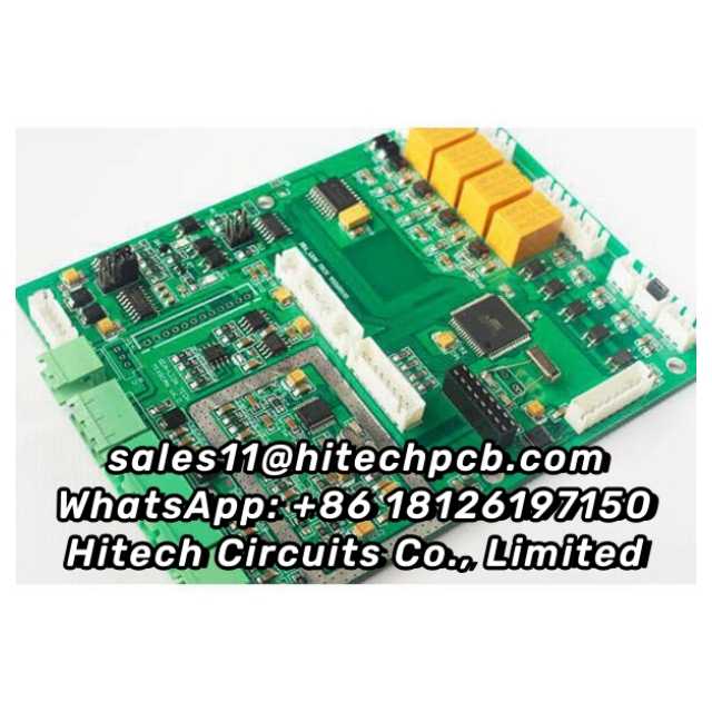
How to reduce Ground Bounce Reduction on PCBAs
1. Minimize return paths
The shorter the return paths, the lower the inductance between components and the ground plane. Therefore, digital components should be placed directly over digital ground areas and mixed-signal devices should be positioned above bridges between digital and analog ground areas, whenever possible.
2. Use short component leads
Using packages with shorter component leads reduces the series inductance. This is also accomplished by using BGAs and vias. Decoupling capacitors should also be used to funnel disturbances to ground as quickly as possible. It is probably a good idea to use these for all IC and transistor ground pins.
3. Use multiple vias
Another way to quickly dissipate disturbances or noise from your circuits is to use multiple vias to route to ground.
4. Offset switching, if possible
The parasitics that cause ground bounce may not be able to be completely eliminated; however, by offsetting switching times, you can minimize the extent or magnitude of the ground bounce.
5. Use slower switching components, if possible
This technique should be used in conjunction with offsets to allow damping to occur prior to the next switching event. This will prevent it from being added to the noise that may be already present.
#pcba #pcbassembly #pcba manufacturer China